二维码
755-83952751
公司總部:廣東省深圳市龍崗區坂田街道雪崗北路2018
號天安云谷產業園一期3棟B座503A
工廠地址:廣東省深汕特別合作區鵝埠鎮同德路與創強
路交匯處

聯繫我們

微信公眾號二維碼
手機版
Copyright © VICFUSE 粤ICP备20045961号 Powered by 300.cn


導航

產品中心
產品中心
VFSMD1210
VFSMD1210
Feature
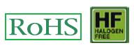
a.RoHS compliant & Halogen Free
b.All high-density boards
c.1210 Dimension,Surface mountable,Solid state,Faster time to trip than standard SMD devices.
d.Operation Current:0.05A~2.00A
e.Maximum Voltage: 6V~60V DC
f.Temperature Range: -45°C to +85°C
Material
Terminal Pad material: Pure Tin
Soldering Characteristics: Meets EIA specification RS 186-9E, ANSI/J-std-002 Category 3
Approval
UL Recognized Pending
TUV Pending
Dimensions
IH=Hold current-maximum current at which the device will not trip at 23℃ still air.
IT=Trip current-minimum current at which the device will always trip at 23℃ still air.
V MAX=Maximum voltage device can withstand without damage at it rated current.(I MAX)
I MAX= Maximum fault current device can withstand without damage at rated voltage (V MAX).
Pd=Typical power dissipated-type amount of power dissipated by the device when in the tripped state in 23℃ still air environment.
RMIN=Minimum device resistance at 23℃ prior to tripping.
R1MAX=Maximum device resistance at 23℃ measured 1 hour after tripping or reflow soldering of 260℃ for 20 seconds.
Termination pad characteristics
Termination pad materials : Pure Tin